
In recent years, the increase in complexity and size of video games has required an evolution in memory management. Sony has promptly responded by developing new storage technology, allowing for faster communication between SoC (System on Chip) and SSD (Solid State Drive) while easing the load on the CPU.
New speed standards
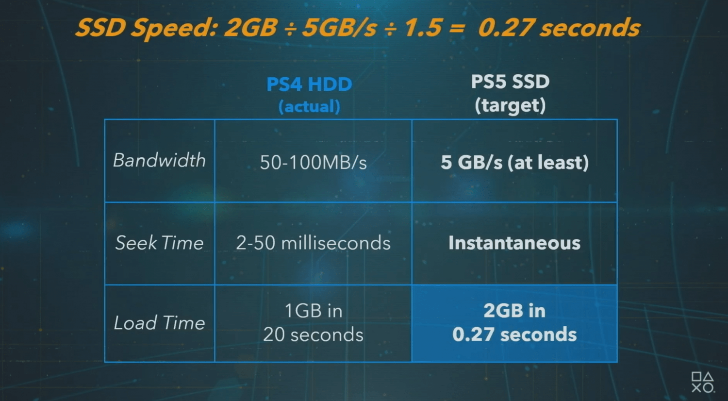
The previous generation of consoles' hard drives took ⅔ of time to search for data and ⅓ of time to load it, so developers were forced to replicate textures and assets (i.e., files or codes containing graphical and structural properties of the game) multiple times within game files, increasing their total size. In order to cope with this problem, RAM was filled with potentially useful data that, in most cases, was not used.
The revolutionary aspect of PS5's SSD is the optimized architecture, which allows textures and assets to be channeled directly into the CPU and GPU pipeline (sequence of instructions to be executed in series), without accumulating excess data in system memory. This allows Sony to reduce RAM capacity and, consequently, production costs. In addition, data is no longer addressed by name, but by ID - a dramatic improvement in search times, now virtually instantaneous, that relieves developers of the need to duplicate game parts.
The key to optimization
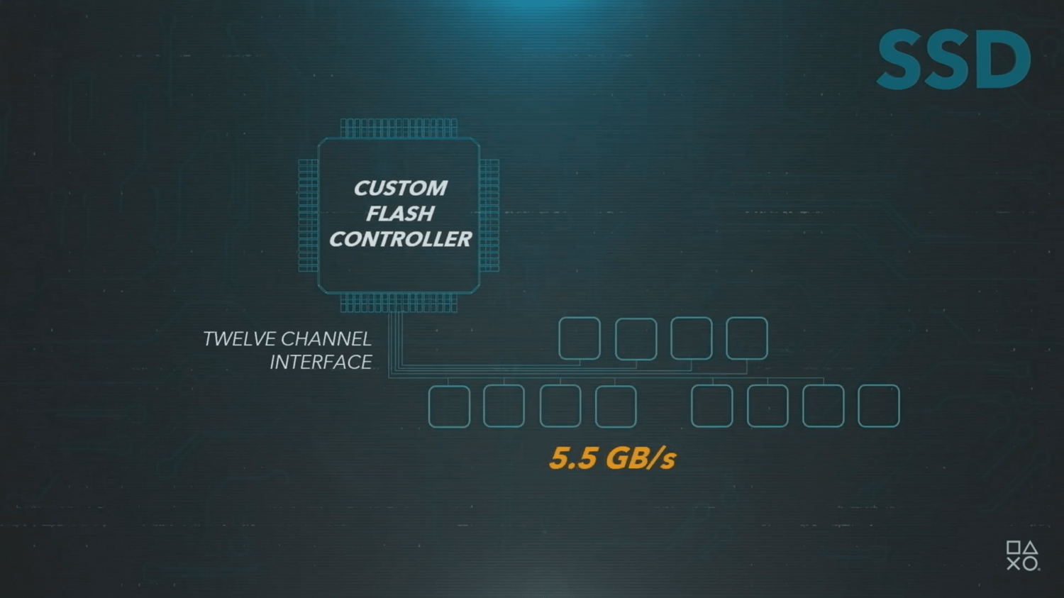
The heart of this structure is an external controller (Custom Flash Controller) with 12 channels, around which Sony has developed its innovative architecture. The Japanese company had to reconfigure the basic system with which the machine processes game data. While in the previous generation was the CPU alone to manage the flow of data between the disk and the system memory, now to act as an intermediary between the two is a controller at the direct command of the processor. This controller is responsible for transferring information from the SSD to the SoC via a PCIe 4.0 port with a bandwidth of 5 GB/s.
Its job is also to control the I/O complex, completely renewed by Sony, inside which there is a DMAC (Direct Memory Access Controller), responsible for addressing data in memory. In addition, the I/O complex is home to two co-processors which, using a decompressor in Kraken technology of the latest generation, save the CPU a considerable workload: without it, it would take 9 Zen 2 AMD CPUs to complete the same decompression operation.
Conclusion
Sony's decision to combine programmable devices and SoCs lays the foundation for an innovative future in consumer electronics. As proof of this, at the beginning of this year a major manufacturer such as AMD also presented its first CPU with integrated reprogrammable devices such as FPGAs (Field Programmable Gate Arrays). These innovations show that in order to reach new standards, it is no longer only computational power that counts, but also the optimization of the system architecture.
Written by Appuhamy Brian Shehara, Marco Vitali e Vittoria Sebastiano from the VGen Engineering Hub


